As regards important applications, there is considerable research and demonstrations involved in the development of thin films of graphene for use as inexpensive substitutes for optically transparent electrically conductive SnIn oxide electrodes presently serving as electrodes in organic solar cells. Another promising area is their use as virtually transparent transistors used to drive computer/telephone display screens. Graphene transistors exhibit very high rates of electron transport, and thus exhibit much faster operation at greatly reduced power consumption. The use of this material for nuclear mediation purposes is clearly advantageous, and is of high interest.
Production of graphene is very difficult; the most common procedures have been involved with the isolation of ~square micron surface area samples isolated from graphite. Recent attempts have shown some success in producing large area samples; these result in the production of near single monolayer deposits of very small graphene particles. Other research has been involved in the chemical reduction of oxides of graphene suspended over membrane pores to yield larger domains of graphene; these may be later transferred to other supports. While these techniques are certainly important, it remains to produce “per se” large surface area, homogeneous, relatively defect-free single monolayer production quantities of pure graphene.
We believe that the present method we have found is an important step forward far realizing this technology.
PROPERTIES
The subject material has the following physical characteristics:
– GIXD spectroscopy of typical bulk samples reveal that the films consist of a dense carbon nanostructure. The new structure is not pyrolytic, as evidenced by domain structures on the order of 30 angstroms, compared with ~200 angstroms for pyrolytic graphite. Further, interlayer spacing is larger (3.48 angstroms) than that of pyrolytic carbon (3.36 angstroms). Some of these preliminary studies indicate that the long distance structure may be altered during the fabrication process. We consider that these results are indicative of a specular reflecting graphite, i.e. a composite of well-formed and homogeneous graphene layers, with the important result that the surface area of the graphene sheets are very large and homogeneous; we have produced sheet areas of several square cm.
Confirmation of this is evidenced by examination of the Raman scattering spectra of the bulk material, material comprising fewer numbers of graphene monolayers, and mono- or near-monolayers of graphene; these non-bulk samples are evidenced by increasing optical transparency at visible wavelengths. The spectra we have measured were made on both SiO₂ supports, and on samples that were free-standing, having been mechanically detached from their support. Measurements were performed under ambient conditions and at a laser frequency of 633 nm.
The spectral behavior of graphene sheets and detached bulk graphite sheets comprised of graphene sheets are well-characterized. Typically, spectra include prominent scattering at ~1580cm⁻¹ and ~2700cm⁻¹. The former wavelength corresponds to the G band, whilst the latter corresponds to the G’ band. The G band corresponds to the the doubly degenerate zone center E2g vibrational mode, and the G’ band corresponds to interaction of the radiation with zone boundary phonons; the latter is forbidden by Raman selection rules, hence it is attributed to boundary defect scattering, and observed only in graphite containing large numbers of layer defects. Further, and most importantly, the characteristic shift in the spectra near 2700cm⁻¹ to higher wavenumbers for the appearance of pure graphene is observed as expected. For the thinnest sheets (near monolayers of graphene), the peak is very sharp and transitional broadening disappears. This is significant as it is known that for more than about five monolayers, the spectra are virtually identical to those of bulk graphite samples.
SEM and TEM electron microscopic analysis yields quite “boring” visualizations, which we consider as further positive evidence of extremely homogeneous, defect-free graphene layers comprising the graphite.
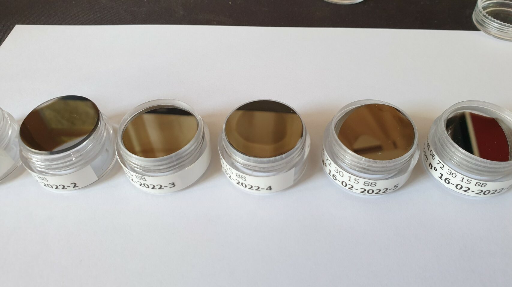
The graphite surface exhibits nearly specular reflectance, at least in the visible region of the spectrum, i.e. they look like pure polished chromium mirror surfaces.
The point electric resistance figures are consistent to that of graphite; i.e. those consistent with the semi-metallic properties of graphite.
The material has no fusion point at atmospheric pressure, but rather sublimes only at temperatures greater than 700°C with oxygen and more than 2000°C without oxygen. (Qualification under investigation)
The material is prepared from a single very low cost organic reactant, upon a simple inorganic support substrate.
The material can be prepared in desired thicknesses; presently from near monolayer graphene, to thicknesses of several microns. Absolute monolayer and larger thicknesses under more controlled conditions are under investigation.
Free-standing samples of the material on the order of 1cm² have been easily isolated.
The material can be produced on a laboratory bench with inexpensive, common equipment. Sample production can be completed in few minute. Extension to high surface area, continuous production is quite evident.
The material is very chemically inert to oxidation and reduction, inorganic and organic solvents, etc., i.e. consult the chemical properties of graphite. As a defect and edge-free material, its chemical stability is naturally increased due to absence of reaction sites on the surface.